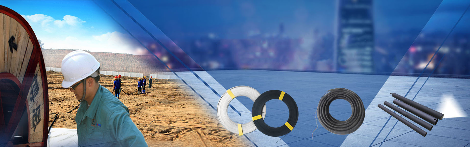
Tel:0539-3712117
First, the trend of localization of electronic materials
By 2016, the proportion of domestic electronic materials is still very low (not more than 10%), and high-end packaging materials are almost blank, which has seriously hindered the development of the domestic electronics industry.
At present, China's advanced electronic high-end packaging market is basically dominated by foreign manufacturers and Taiwanese manufacturers, ASE, Amkor, SPIL, etc. occupy the majority of market share, mainland China suppliers only Jiangyin Changdian, Huatian Technology, Tongfu Microelectronics A few of them, their market share is also very small.
The package test is a downstream process of integrated circuit manufacturing. The integrated circuit package is a process of further processing the wafer to be tested to obtain a separate chip. The purpose is to add a function for connecting the contacts of the chip to the external circuit, such as adding a reference. The foot is connected to an external circuit such as a PCB. At the same time, the package can add a "protective shell" to the chip to protect the chip from physical or chemical damage. At the end of the packaging process, the electrical function of the chip is confirmed.
China's mainland is currently entering a period of intensive construction of semiconductor production lines. The demand for semiconductor equipment and materials is growing rapidly. The annual demand for the mainland is expected to exceed US$20 billion. Domestic equipment and materials manufacturers are welcoming large opportunities for import substitution. With the failure of Moore's Law, the development of integrated circuits is particularly dependent on innovative breakthroughs in advanced electronic packaging technology, so advanced electronic packaging materials will play a vital role.
On the other hand, with the implementation of national strategies such as "Made in China 2025" and "Internet +", smart manufacturing and industrial upgrading will lead to a huge IC market. This means that electronic packaging materials will face a wide range of industrial opportunities. The integrated circuit is developing toward miniaturization, thinning, high performance, multi-functionality, high reliability, and low cost, and the packaging of integrated circuits has evolved from the original two-dimensional to more dimensional.
"Materials are the pain of China's electronics industry." With the development of China's economy, the localization of electronic materials is imperative. The next 5-10 years will be the period of rapid development of China's electronic materials, with challenges and opportunities coexisting.
Second, the development of flexible electronic materials has broad prospects
Since the "Twelfth Five-Year Plan", flexible electronic technology has flourished, and the flexible electronic devices that have been developed from this have been in the ascendant. Smart wearables are an important application. Flexible electronic devices have emerged in new energy equipment, disease prevention and treatment, smart phones, large-size display screens, aerospace and other fields. Flexible portable energy storage batteries, flexible supercapacitors have preliminary products; biocompatible flexible sensors play a preliminary role in heart disease monitoring, pulse induction, brain wave detection, etc.; the popular millet bracelet, due to its beauty Cheap, can be said to be the first wearable device into the lives of Chinese people, the main functions include viewing the amount of exercise, monitoring the quality of sleep, smart alarm wake up, etc., can also identify more sports through the cloud; earlier Google launched by the United States Google Glass, Apple's smart watches, etc. have also caused a lot of repercussions in the market; organic light-emitting diodes have also been initially applied in the field of display illumination; in the aerospace field, flexible electronic devices are controllable and space-saving. Some applications have also been obtained.
Currently in the field of printed electronics, commonly used flexible materials are usually organic materials, including PI (polyimide), PET (polyethylene terephthalate), PEN (polyethylene naphthalene), PEI (polyether amide) Amine), transparent conductive polyester, and the like. By 2030, the performance of existing organic materials will be greatly improved. For example, the current organic semiconductor mobility maximum value of 1cm2V-1s-1, when we can develop an organic semiconductor comparable to single crystal silicon mobility of 103cm2V-1s-1. Current research hotspots such as flexible materials, two-dimensional materials such as graphene and molybdenum sulfide, and one-dimensional materials such as carbon nanotubes and nanowires will mature. And new inorganic flexible materials will also enter our application.
Thanks to the development of materials technology such as organic light-emitting diodes, flexible display technology will surely be developed in depth and extensively in the next 30 years. It will not only be limited to organic materials, but also exhibits diversified and intelligent features. The flexible display screen will enter the market and even become the mainstream product of the display screen. For example, a large-sized flexible display screen, a display screen for everyday flexible electronic products, and the like.